How Transistors Work: From Sand to Silicon Supercomputers
Basic Brain
Engineering & Science • November 09, 2026
How Transistors Work: From Sand to Silicon Supercomputers
Look down at your phone, laptop, or whatever device is rendering these words right now. Beneath the glowing glass sits a piece of crystalline silicon no larger than a postage stamp.
Inside that microscopic chip are tens of billions of microscopic switches—each turning on and off billions of times every single second without making a sound, moving a mechanical part, or emitting a puff of smoke.
Those switches are transistors, arguably the single most important human invention of the 20th century. Without them, there are no computers, no internet, no smartphones, and no artificial intelligence.
In this deep dive, we're stripping away the jargon to understand the pure physics and engineering behind how a transistor works—from voltage and current to the atomic dance of semiconductors.
1. The Triad of Electricity: Voltage, Current, and Resistance
Before we can appreciate how a transistor directs electric current, we have to understand the fundamental laws that govern moving charges.
Every electric circuit relies on three core properties:
- Voltage (, measured in Volts): Electric potential pressure. It is the force that "pushes" electrons through a medium.
- Current (, measured in Amperes): The actual rate of flow of electrons passing through a cross-section per second ().
- Resistance (, measured in Ohms ): The opposition to that flow caused by atomic collisions and material constraints.
These three quantities are locked in an unbreakable relationship known as Ohm's Law:
Why Resistors Matter in Transistor Circuits
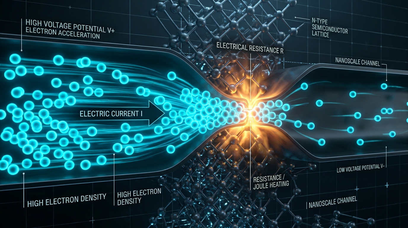
When high voltage pushes electrons through a conductor without resistance, the current spikes infinitely (a short circuit), generating immense heat that destroys delicate semiconductor junctions.
Engineers use resistors before the base or gate of a transistor to safely choke the incoming current, keeping the voltage within the exact threshold needed to trigger switching without vaporizing the component.
2. What Is a Semiconductor? (Doping Silicon)
Conductors like copper let electrons flow effortlessly. Insulators like rubber or glass lock their electrons in tight bonds so nothing moves.
Silicon is special: it is a semiconductor.
An atom of silicon has 4 valence electrons in its outer shell. In a pure silicon crystal, each atom shares its 4 electrons with 4 neighboring atoms, forming flawless covalent bonds. Because all electrons are locked tightly into this crystalline lattice, pure silicon is actually a mediocre conductor at room temperature.
To turn silicon into an active electronic element, scientists perform a process called doping—introducing microscopic traces of impurities:
- N-Type Silicon (Negative): Silicon is doped with elements like phosphorus or arsenic, which have 5 valence electrons. Four of them bond with silicon, leaving one extra electron free to float around. This material now has an abundance of free negative charge carriers.
- P-Type Silicon (Positive): Silicon is doped with elements like boron, which have only 3 valence electrons. When it bonds with neighboring silicon, an empty space—an electron "hole"—is left behind. These holes behave like positively charged particles seeking electrons.
3. The PN Junction: Creating the One-Way Gate
When you bring a block of P-type silicon and N-type silicon into direct atomic contact, something extraordinary happens at the boundary.
The free electrons from the N-side naturally rush across the border to fall into the vacant holes on the P-side.
As they do, the N-side near the border loses electrons and becomes slightly positively charged, while the P-side gains electrons and becomes slightly negatively charged.
This creates a localized barrier called the Depletion Region:
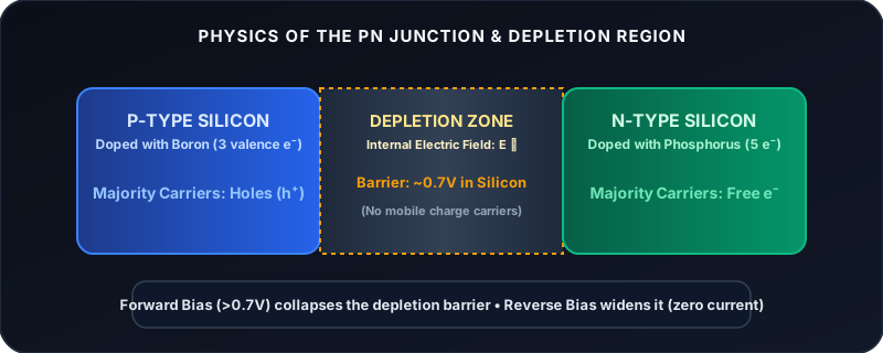
This internal electric field pushes back against further electron flow, sealing the gate shut.
- Reverse Bias (Positive to N, Negative to P): The external voltage pulls electrons and holes even further apart, widening the depletion zone. Zero current flows.
- Forward Bias (Positive to P, Negative to N): Once your applied voltage overcomes the internal threshold (about 0.6V to 0.7V for silicon), the depletion zone collapses, and current surges across freely. This two-terminal device is a diode.
4. The Transistor: From Diode to Switch & Amplifier
A transistor takes this concept one step further by sandwiching three layers together: either N-P-N or P-N-P.
Let's focus on the classic NPN Bipolar Junction Transistor (BJT), which has three terminals:
- Emitter (E): Injects electrons into the device.
- Collector (C): Collects the electrons and sends them out to the load circuit.
- Base (B): An ultra-thin middle layer that acts as the control valve.
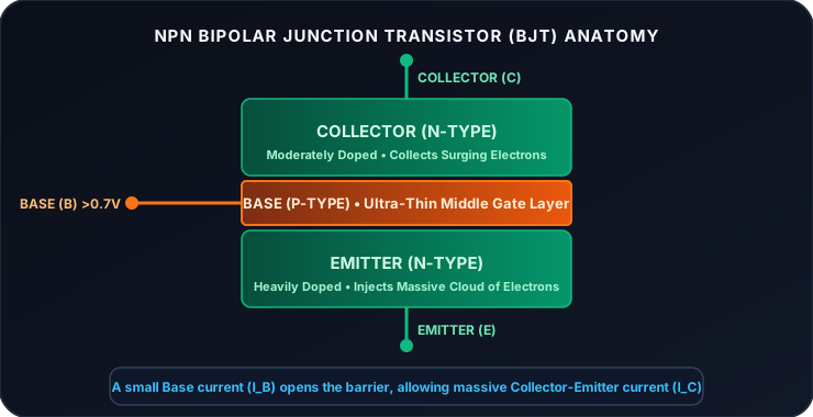
How the Switching Works
If you connect a voltage source between the Collector and Emitter, no current flows because one of the two internal PN junctions is reverse-biased. The switch is OFF.
However, apply a tiny voltage (just 0.7V) and a trickle of current into the Base terminal, and the barrier drops. Because the middle P-layer is microscopically thin and lightly doped, over 99% of the electrons surging from the Emitter overshoot the Base and get swept straight into the Collector!
- A tiny current at the Base opens the floodgate for a huge current between Collector and Emitter.
- Turn off the Base current, and the main current stops instantly.
The Transistor Rule: A small input signal controls a large output flow. This allows the transistor to act either as a binary switch (digital 0 or 1) or an amplifier (analog audio/radio signals).
5. BJT vs. MOSFET: The Modern Microprocessor Standard
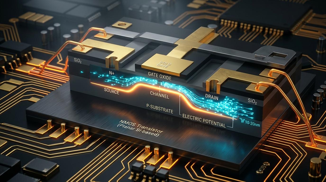
While BJTs ruled early electronics, modern computer microprocessors use a variation called the MOSFET (Metal-Oxide-Semiconductor Field-Effect Transistor).
Instead of using a continuous base current to keep the valve open, a MOSFET uses a tiny insulated capacitor plate called the Gate. When voltage is applied to the Gate, its electric field attracts a conductive channel of electrons underneath the insulator, bridging the Source and Drain.
Because the Gate is electrically insulated by a microscopic layer of silicon dioxide, zero static current flows into the gate. This drastically slashes power consumption and heat generation, allowing engineers to pack over 100 billion MOSFETs onto a single thumb-sized die!
| Metric / Feature | Bipolar Junction Transistor (BJT) | MOSFET (Field-Effect Transistor) |
|---|---|---|
| Control Signal | Current-driven (Base current ) | Voltage-driven (Gate electric field ) |
| Input Impedance | Moderate () | Extremely high () |
| Power Consumption | Higher (Base draws continuous current) | Minimal (Only consumes energy when switching) |
| Switching Speed | Fast, but limited by carrier storage | Ultra-fast (nanosecond to picosecond scale) |
| Primary Domain | High-power RF, analog amplifiers, sensors | Microprocessors, RAM, digital logic gates, GPUs |

6. Watch the Breakdown & Visual Demonstrations
Seeing dynamic electron movement in real-time makes the physical intuition click. Watch this excellent visual breakdown illustrating the internal junction kinetics:
Reference & Community Channel
For more deep dives into mechanical physics, electronics, motors, engines, and fundamental science, subscribe and explore:
- 🎥 Basic Brain on YouTube (@basicbraincut) — Visual explanations of how real-world machines, electronics, and historical engineering marvels work.
7. Key Takeaways
- Electricity is a team: Voltage is the push, current is the flow rate, and resistance governs how much passes through ().
- Silicon needs a boost: By doping pure silicon with phosphorus (N-type) or boron (P-type), we unlock mobile charge carriers.
- The PN junction is the foundation: It naturally creates a depletion barrier that allows one-way current flow.
- Transistors are solid-state valves: A small electrical input at the Base or Gate controls a massive flow from Collector/Drain to Emitter/Source.
- MOSFETs power the world: Because they are controlled purely by an electric field without needing constant current flow, they form the bedrock of all modern computing and AI chips.
Written & curated for the Basic Brain engineering library. Have a question or a topic you'd like us to dissect next? Drop your thoughts in the comments below!